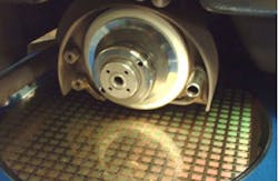
Silicon-wafer manufacturing uses large volumes of expensive, ultrapure water for cooling, lubricating and flushing of wafer cuttings generated during slicing, back-grinding and die-sawing operations. Most these cuttings are very hard and sharp-edged, in addition to constituting a fine colloidal-solids load.
Issues and concerns related to wafer-process wastewater include that not reusing or recycling high volumes of ultrapure water is expensive and that traditional gravity-filtration methods for adding organic coagulants or flocculants to wastewater can contaminate an ultrapure water stream. On the other hand, concentratingTubular-membrane filtration (TMF) is a cross-flow technology that removes in a single step the particulate and colloidal solids load from wafer-process wastewater streams. This filtration technology does not require pretreatment or organic coagulants or flocculants addition, and it renders the resulting ultrapure water reusable. TMF exhibits a unique membrane and substrate surface topography that results in very high resistance to abrasive solids.
A recent advance in TMF filters is a specially formulated, high-flux 20nm-rated tubular membrane, meant to remove virtually all particulate loads, including the very fine colloidal particulate often found in semiconductor water streams. This membrane was developed in response to water-treatment system makers asking for membrane products tailored to the semiconductor industry.
Boules done first
The first step in manufacturing silicon wafers is making the monocrystalline boules. A boule is a single crystal ingot produced by synthetic means. A boule of silicon is today the starting point for most integrated circuits.
In this case, ultrapure silicon is drawn into long cylindrical single crystal boules, up to 12 inches in diameter and several feet long. This is done by slowly pulling a metal rod — with a seed crystal on the end — vertically upwards from a liquid surface of molten silicon in a crucible. A similar process is used to manufacture sapphire boules for semiconductor devices such as LEDs.
Silicon boules are cut to make the wafers: sawn across the diameter "salami style," and notched or flattened on the edge to identify the crystal plane alignment for subsequent processes. For photovoltaic applications, the boule may be squared-off on all sides. Slicing is done with diamond-impregnated wire saws, plain-wire saws and abrasive slurry containing silicon carbide or diamond, and diamond ID saws (which have their cutting-edge on the inner diameter of the saw blade).
Ultrapure water cools the operation and flushes away cuttings without contaminating the wafers.
Next come silicon ingots
Sometimes, cast polycrystalline silicon ingots, rather than the monocrystalline boules, are used for integrated circuits. They are lower cost and generally used in larger-scale semiconductor devices such as solar cells. These are most often trimmed and cut into rectangular "bricks," then sliced into individual wafers using a wire saw.
Some organic wetting agents and lubricants might be present in very small concentrations in wastewater from these operations.
The backgrinding operation, sometimes called thinning, is where the silicon wafers, 20 to 30cm in diameter, are reduced in thickness from approximately 750µ to around 20 to 30µ, sometimes considerably less. Grinding wheels, impregnated of various grades of abrasive (typically diamond) are used. The initial wafer thickness ensures good stability and strength during the formation of the integrated circuits within the top surface. While the wafer is being ground, it is secured with a special adhesive film.
Chemical mechanical planarization (CMP) is done on the top surface. A very tiny portion of the total semiconductor liquid waste is produced from CMP operations.
One object of backgrinding is to reduce the wafer thickness to minimize the "packaged" dimensions. It also improves microchip cooling efficiency as heat can be more readily conducted away into the package heat sink. The bulk of the material from the original boule is removed by backgrinding.
Copious amounts of ultrapure water are used for cooling and flushing during grinding. In general, negligible amounts of organic chemical additives should be in the waste slurry from backgrinding. This is a good application for tubular-membrane filtration.
Now saw the dies
The die-sawing operation, also called "dicing" or "singulation," is where the silicon wafer is cut into individual microchips. This is done either before or after backgrinding. Typically, the cutting tool is a metal disc impregnated with diamond particles. The wafer is held in place with an adhesive tape that dissolves to release the individual microchips after dicing.
Wastewater from dicing operations generally has much lower solids content than backgrinding waste. It is more likely to contain organic additives such as wetting agents and lubricants, used to reduce the chances of chipping on the face where the actual electronic device is located. The addition of organic additives can be an issue. Organic additives are likely to foul membrane filters, leading to frequent chemical cleaning to maintain performance. Hollow-fiber microfilters may also work for dicing wastewater due to its low solids content.
Process wastewater derived from microelectronics device-making is typically a spent-fluids mix such as described above, plus other grinding, lapping and polishing operations, including intermediate washing steps. This wastewater is essentially ultrapure water, silicon cuttings and spent abrasive. Small amounts of lubricant and surfactant/wetting agent may also be present, particularly for sawing operations.
Solids contained within the wastewater are mostly a mixture of facetted silicon cuttings and spherical colloidal silica. The silicon cuttings partially oxidize to silica to a depth of a few nanometers in the wastewater. Silica is likely to be present in small percentages in ionic, polymeric and colloidal forms. Silica fouling is to be expected and occasional caustic (or hydrofluoric acid) cleaning procedures can effectively restore membrane performance.
In microelectronics making are also found spent coolants, wash water, abrasive slurries from CMP and solar-cell manufacture, and mobile-device screen-glass polishing waste. Some facilities use more lubricating and wetting-agent additives than others and, as a result, might not have such high value water to reclaim. Mixed waste streams can also be problematic.
Succeed at tubular micro-filtration
A successful tubular micro-filtration application must avoid rapid mechanical pore blinding. Therefore, the membrane pore-size rating is smaller than the smallest particle size in the waste stream. A total organic carbon (TOC) analysis will indicate the membranes’ likely organic fouling rate and the chemical-cleaning frequency required. These two measurements give good indication of the practical performance and chemical-cleaning type and frequency required.
A growing concern related to semiconductor production is use of very toxic materials such as gallium arsenide (GaAs). Microelectronics based on GaAs are inherently low-noise, particularly in high-frequency applications, such as microwave communications, light-emitting diodes, laser devices and super-computer components. Concerns about GaAs escaping to the environment are based on potential reactions that can produce carcinogenic and even nerve-agent-like compounds. Research is continuing. TMF can be an effective method for removal of GaAs solids, regardless of whether chemical or electro-chemical pretreatment is applied.
Fluoride discharge is also a concern. Increasingly stringent restrictions on fluoride discharge in the areas where semiconductor manufacturing plants flourish presents another application for cross-flow microfiltration. Precipitation, by one or more chemical processes, can remove fluorides down to very low residual levels. These processes can be augmented with TMF filtration to remove the precipitates and improve the overall fluoride removal performance.
Implications globally
Efficiency and limiting waste are important to all semiconductor-industry stakeholders, including local communities. The largest wafer-making operations are in Asia where stringent discharge limits are emerging. In some instances, water consumption constraints are limiting production expansion. These trends emphasize improved, sophisticated and efficient process-water treatment and recycling.
Porex TMF products are used in silicon-wafer manufacturing wastewater treatment worldwide. In one example, a memory-device manufacturer in Korea says the TMF-based system meets filtration and reclamation objectives while saving about $1 million per year.
The 20nm membrane tubes used have been engineered to meet the highest standards of the filtration industry and were subjected to extensive performance and durability testing to ensure long and efficient operation in this challenging filtration application.
Alan Walton, as director of innovation and technology at Porex Filtration, joined the newly formed Porex Filtration Group in 2005 to develop products and manufacturing methods for the industrial filtration business. This position requires a knowledge mix that includes market analysis, product design and development, manufacturing technology development and product applications support.
Porex Filtration Division provides unique solutions to high-solids filtration and separation problems with microfiltration and ultrafiltration systems. Industrial filtration applications include water & wastewater, paints, inks, polishing slurries, catalyst recovery, trap filtration, pulp & paper, metal finishing and completion fluids.


